🔬 Bridging Microelectronics and Photovoltaics
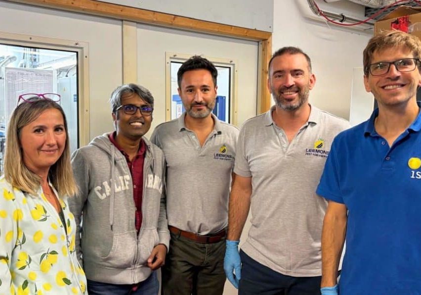
In this interview, a research engineer from CEA-Leti (Grenoble) presents CEA’s role in the LEEMONS project and explains how advanced ion implantation technologies are being adapted to support next-generation photovoltaic innovation.
CEA-Leti is a leading European research institute in microelectronics and nanotechnology. Within LEEMONS, its expertise in ion implantation and materials engineering plays a central role in developing buried amorphous layers in silicon.
▶️ Watch the Interview – Frederic Milesi
⚙️ What is Ion Implantation?
Ion implantation consists of introducing ionized atoms or molecules into a material in order to modify its properties.
This process can alter:
- Physical properties
- Mechanical behaviour
- Electrical characteristics
- Optical properties
In microelectronics, ion implantation is a well-established and highly controlled process. Within LEEMONS, this technology is being adapted to serve new objectives in the photovoltaic domain.
🧪 CEA’s Role in LEEMONS – Work Package 2 Leader
CEA-Leti leads Work Package 2, dedicated to:
The fabrication of buried amorphous silicon layers using physical masking techniques.
This work involves several major technical challenges:
1️⃣ Fabrication of buried amorphous layers
Developing processes to create controlled amorphous regions inside crystalline silicon.
2️⃣ Integration of physical masks
Introducing physical masks into ion implantation equipment to enable discontinuous implantation patterns.
3️⃣ Adapting microelectronics equipment
Processing square photovoltaic wafers in equipment originally designed for 300 mm round microelectronics wafers.
These adaptations require innovative engineering solutions to bridge two industries with different standards and constraints.
🚀 Technical and Industrial Perspectives
Beyond photovoltaics, the developments achieved in LEEMONS may also have implications for microelectronics.
In particular, the use of physical masks could potentially enable:
- Patterning without conventional photolithography
- Reduced manufacturing costs
- Alternative approaches for relaxed technological nodes (micron-scale technologies)
This cross-fertilisation between photovoltaic and microelectronics industries represents one of the project’s added values.
🤝 A Multi-Partner European Collaboration
The interview also highlights the strength of the LEEMONS consortium:
- Research centres
- Start-ups
- SMEs
- Industrial partners
Each organisation brings different methodologies and constraints, but works toward a common objective: advancing photovoltaic efficiency through innovative electron multiplication approaches.
🌍 About LEEMONS
LEEMONS (Low-Energy Electron Multiplication On Nanostructured Solar Cells) is a Horizon Europe project funded by the European Union under Grant Agreement No. 101172870.
The project aims to demonstrate an innovative electron multiplication phenomenon capable of overcoming thermalisation losses in silicon solar cells, potentially opening a new pathway toward higher-efficiency photovoltaic technologies compatible with existing manufacturing lines.
🇪🇺 Funding Acknowledgement
Funded by the European Union. Views and opinions expressed are however those of the author(s) only and do not necessarily reflect those of the European Union or CINEA. Neither the European Union nor the granting authority can be held responsible for them.


